
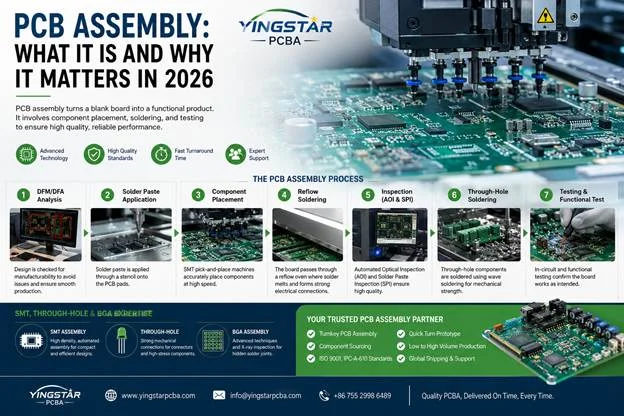

PCB assembly turns a blank board into a functional product. PCB assembly involves component placement, soldering, and testing the completed board. This explains how the process works and why cost and quality vary.
Every device on your desk now. Laptop, router, phone charger. Began as a plain green board that had no clue what purpose it would serve. I see that PCB assembly is the step that changes that. PCB assembly is the process of placing resistors, capacitors, connectors, and chips on a printed circuit board, then soldering them. Hence, the board becomes a working circuit instead of just a strip of fiberglass and copper.
For hardware teams, PCB assembly isn’t a minor detail. In fact, in most cases, PCB assembly is the biggest factor in whether a product ships on time and works in the field. This guide breaks down the process, major assembly methods available, and the details that separate a stress-free build from an expensive one.
What Is PCB Assembly (PCBA)?
PCB assembly, often shortened to PCBA, refers to the full sequence of populating a bare board with electronic components and forming the solder joints that hold them in place, followed by inspection and functional testing. It differs from PCB fabrication, the earlier step of etching copper layers into the board itself.
A PCB fabricator makes the board. An assembler puts the parts on it. Some companies like to give those two jobs to vendors. However, I see a growing number of companies offering turnkey PCB assembly now. PCB assembly is when a company takes responsibility for creating the PCB, sourcing the necessary components, and placing everything correctly on the board in one location. This construction method has quickly become popular with most new hardware design firms. It separates blame between the team that created the board and the team that assembled it. It removes blame over who is at fault.
The PCB Assembly Process, Step by Step
A production‑grade PCB assembly run follows a steady order, but different shops may use different equipment.
Design for Manufacturing and Assembly (DFM/DFA)
Before any component touches the board, the design is checked against the manufacturer’s real-world capabilities—trace widths, pad sizing, component spacing, and fiducial marker placement. Catching a spacing issue here costs almost nothing. Catching it after the first production run costs a re-spin and weeks of schedule slip. Any assembler worth using will run this check even if you don’t ask for it.
Solder Paste Application
A laser-cut stencil sits over the bare board, and solder paste gets applied through its openings onto the exposed copper pads. Paste volume and stencil thickness matter more than most first-time designers expect — too little paste, and you get weak joints; too much and you risk bridging between fine-pitch pins.
Component Placement
This is where surface mount technology (SMT assembly) does the heavy lifting. Pick-and-place machines lift components from reels and set them onto the pasted pads with high-speed vacuum nozzles, often placing tens of thousands of parts per hour on modern lines. Through-hole components — connectors, larger capacitors, anything that needs mechanical strength — still get inserted manually or with automated insertion equipment and soldered separately, usually by wave soldering.
Reflow Soldering
The board goes into a reflow oven. The oven heats the board following a careful temperature schedule. The solder paste melts. The solder paste wets the pads. The component leads are soldered. Then the board is reflowed. The solder paste solidifies, making an electrical connection. If your temperature schedule isn’t right, you see the board starting to warp, leaving its joints. The solder paste moves the solder away from a pad and causes a component to slide.
Inspection and Testing
After reflow, AOI inspects each board for missing components, improper alignment, and solder defects. Most production lines also use solder paste inspection before placement to verify solder paste height and volume. This ensures proper solder paste application and lets operators replace stencils when wear is detected at this pre-placement stage, preventing defects downstream. From there, boards usually move on to in‑circuit testing or functional testing. These tests confirm that the assembled product does what it should, not that the solder looks clean.
SMT vs. Through-Hole: Choosing the Right Assembly Method
Most modern boards use a mix of both, not one exclusively:
- SMT assembly: This design fits high component density. It works well for automated high-volume production. It is the choice for anything with fine-pitch ICs or BGA packages.
- Through-hole assembly provides stronger mechanical bonds, which matters for connectors, switches, and parts that take physical stress—think anything a user plugs a cable into repeatedly.
- BGA assembly: Ball grid array packages deserve a mention because they solder underneath the component itself, hidden from view. As a result, X-ray inspection is the reliable way to verify joint quality.
If your board only needs passive components and simple ICs, pure SMT keeps costs down. Anything with connectors or components under mechanical load needs through-hole in the mix; no way around it.
What Drives PCB Assembly Cost and Lead Time
Cost isn’t just about board size or layer count. A few factors move the needle more than people expect:
- Component sourcing. Parts on allocation or nearing end-of-life can add weeks to a build, no matter how fast the assembly line runs.
- Board complexity. Fine-pitch BGAs, mixed SMT/through-hole builds, and high layer counts all slow down programming and setup time, even before the first board runs.
- Volume. Prototype PCB assembly runs (typically under 100 units) carry a much higher per-unit setup cost than production runs in the thousands, since stencil setup and machine programming get amortized across fewer boards.
- Testing requirements. Functional test fixtures and in-circuit test development take real engineering time, and that cost shows up whether you’re building 50 units or 50,000.
A quick-turn PCB assembly service can compress prototype lead times to a few days, which is worth paying for when you’re validating a design — but it’s not the number to optimize for once you move into steady production, where unit cost and consistency matter more than speed.
Working with an Electronic Component Sourcing and PCB Assembly Manufacturer
Choosing a partner comes down to a handful of concrete questions, not just a quote. Does the printed circuit board assembly manufacturer purchase? Do they keep your parts in stock, or do they want a consigned kit? What type of qualifications does the manufacturer possess? IPC-A-610 class ratings, ISO 9001. If your industry is highly controlled, do they have ISO 13485 for the medical industry or AS9100 for printed circuit board assembly in aerospace? What’s their actual defect rate on a comparable build, not just their marketing copy?
Industrial control PCBA and automotive PCB assembly in particular tend to demand tighter traceability — serial-level records linking components, machine parameters, and test results back to a specific build. That level of documentation costs more upfront, but it’s what lets you trace a field failure back to a root cause instead of guessing.
Conclusion
PCB assembly is the moment when a design either becomes a product or turns into a source of ongoing headaches. The difference usually comes down to DFM discipline, early sourcing decisions, and an assembler that treats inspection as more than a formality. Whether you are running a prototype batch or scaling to high-volume production, the fundamentals stay the same: verify the design before it hits the line, choose the right mix of SMT and through-hole for your components, and don’t skip testing just to save a few days on the schedule.